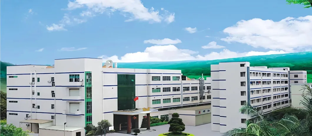
Low-Power MCU & Soc Chips for IoT Devices Arm/Risc-V Architecture Ideal for Smart Home & Wearable Applications

Customization: Available
Type: Rigid Circuit Board
Dielectric: FR-4

Product Description

Overview
Workshop
Detailed Photos
Product Parameters
Certifications
Customers
Packaging & Shipping
FAQ
Basic Info.
Model NO. pcb
Material Complex
Flame Retardant Properties V0
Mechanical Rigid Rigid
Processing Technology Electrolytic Foil
Base Material Aluminum
Insulation Materials Organic Resin
Model PCB
Brand OEM
PCB Layer 1-26 Layers
Solder Mask Green
Silk Screen White
Surface Treatment HASL
PCB Assembly Type SMT and DIP
PCB Service One Stop Service
Small Orders Accepted
Copper Thickness 1oz
Board Thickness 1.6mm
Lead Time 12-20 Days
Transport Package Vacuum+Carton Packing
Specification RoHS, ISO9001, UL, SGS
HS Code 8534009000
Production Capacity 20000 Square Meter/Mon
Packaging & Delivery
Package Size 20.00cm * 30.00cm * 20.00cm
Package Gross Weight 0.500kg
Product Description
Multilayer PCBA Manufacturer with ISO UL Certification for Single Double PCB Assembly, OEM ODM Services for Consumer Electronics, Automotive, and Medical Applications
We are a leading PCB manufacturer in China with a facility area of more than 40,000 square meters and 1000 professional staff. We served customers in over 40 countries from various electronic industries, over 70% of products are exported to America, Europe and other Asia Pacific countries. We have obtained ISO9001 certificates, UL Certification, and all products meet RoHS compliance.
40,000+
Square Meters Facility
1,000+
Professional Staff
40+
Countries Served
100%
On-Time Delivery Rate

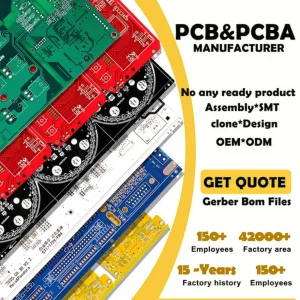
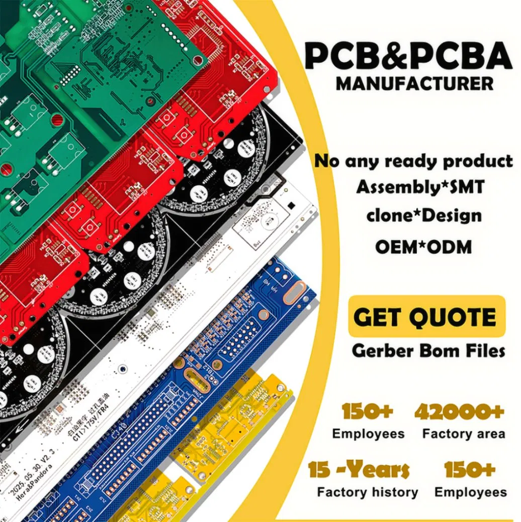
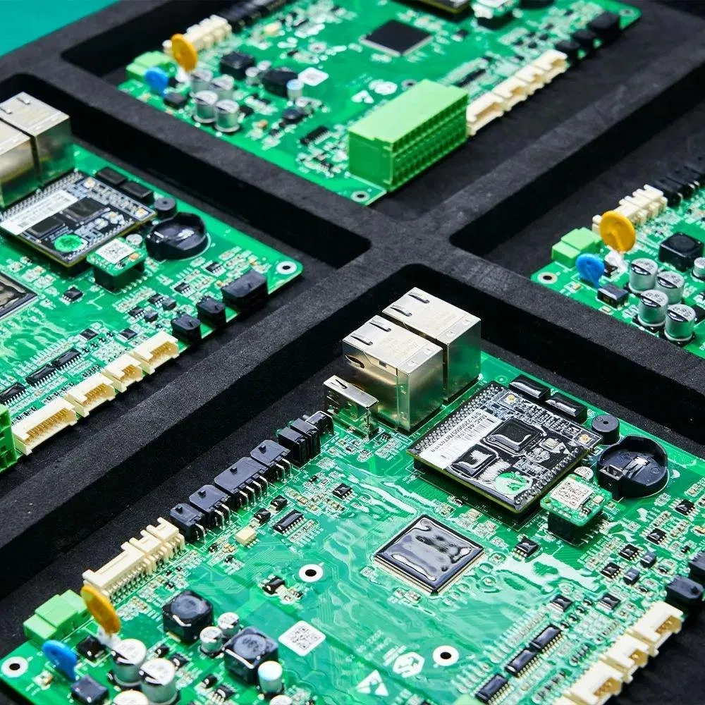
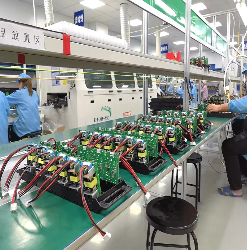
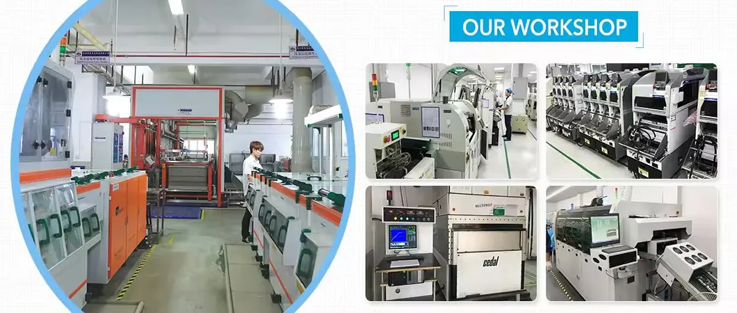
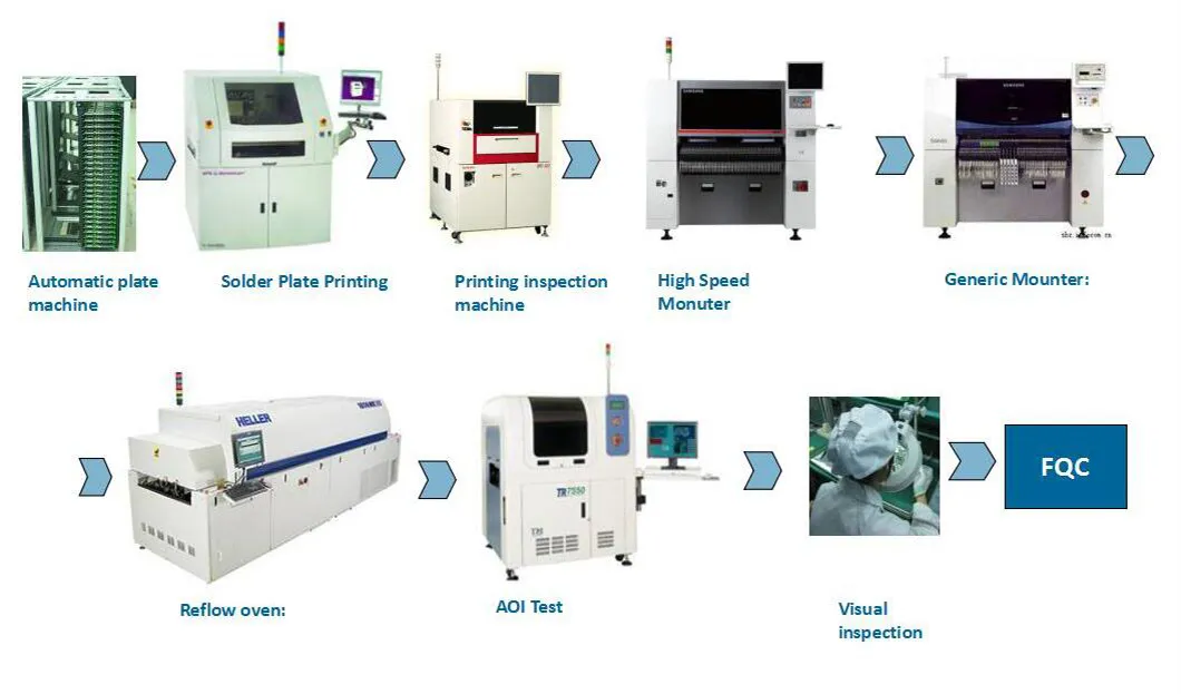
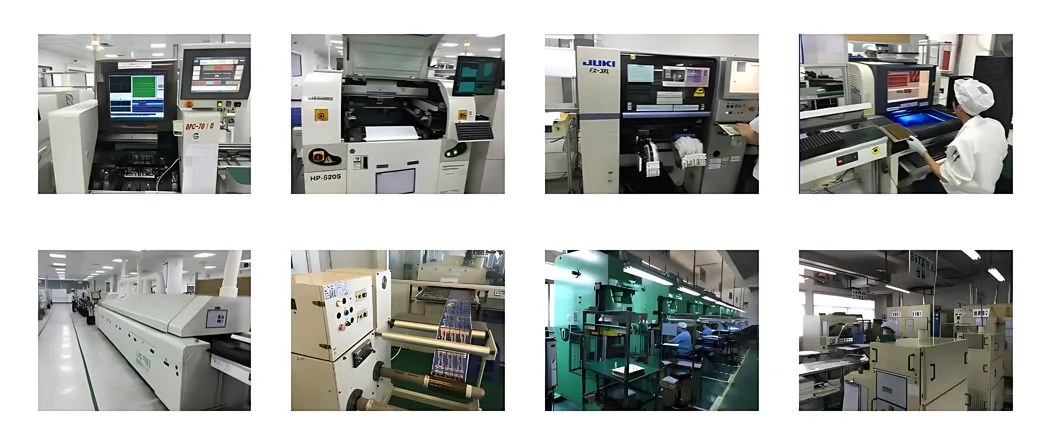
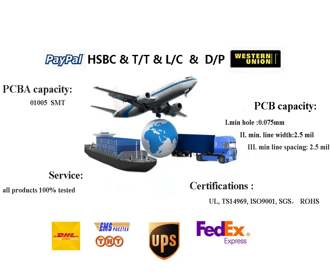
★ One-Stop PCB & PCBA Solution to meet diverse customer demands.

We can meet all your PCB manufacturing needs, including High multilayer PCB, Aluminum based PCB, HDI PCB, Rigid-flex PCB, heavy copper PCB, and PCB assembly. Our products are widely applied in telecom, industrial control, power electronics, medical instruments, security electronics, aerospace, and more.
We pride ourselves in providing superior service as this component is the true heart of who we are. Whether the deadline is for a quote, production, or shipping and delivery, we meet it 100% of the time. We sincerely value long-term relationships with our customers and take responsibility for their longevity and success to remain competitive in a tough market.
IoT Device Applications
Workshop
-- Factory Tour --
Factory Tour
-- Equipments --
Equipment Display 1
Equipment Display 2
Detailed Photos
-- Products Show --
PCB Showcase 1
PCB Showcase 2
Product Parameters
-- Parameters & Data Sheet --
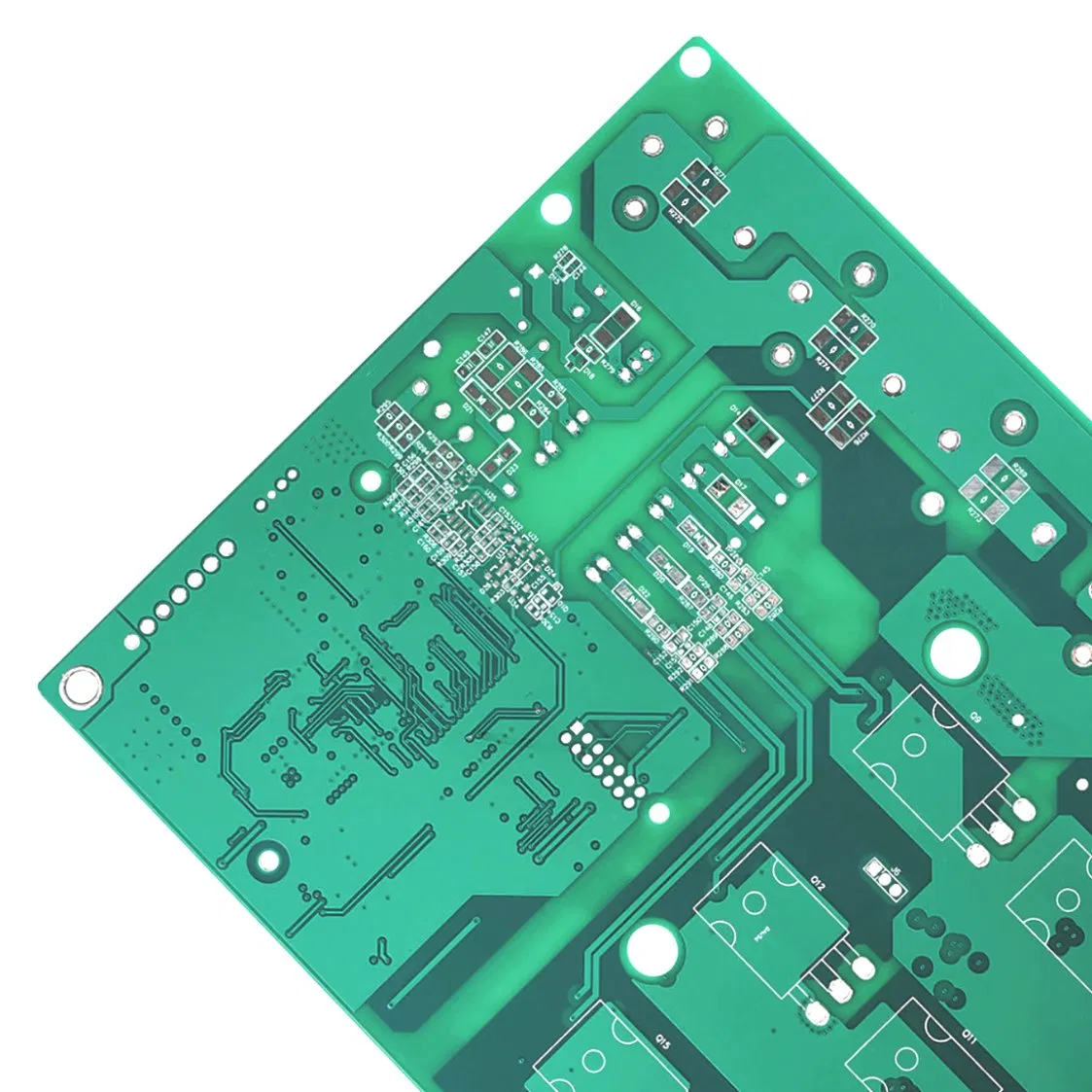
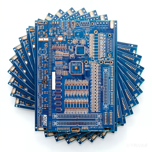
PCB Manufacture Capability
Item Manufacture Capability
Layers 1-26 Layers
HDI 2+N+2
Material Types Fr-4, Fr-5, High-Tg, Aluminum Based, Halogen Free, Isola, Taconic, Arlon, Teflon, Rogers
Max. Panel Dimension 39000mil * 47000mil (1000mm * 1200mm)
Outline Tolerance ± 4mil (± 0.10mm)
Board Thickness 8mil-236mil (0.2 - 6.0mm)
Board Thickness Tolerance ± 10%
Dielectric Thickness 3mil-8mil (0.075mm-0.20mm)
Min. Track Width 3mil (0.075mm)
Min. Track Space 3mil (0.075mm)
External Cu Thickness 0.5 OZ - 10 OZ (17um - 350um)
Internal Cu Thickness 0.5OZ - 6OZ (17um - 210um)
Drilling Bit Size (CNC) 6mil-256mil (0.15mm - 6.50mm)
Finished Hole Dimension 4mil-236mil (0.1mm - 6.0mm)
Hole Tolerance ± 2mil (± 0.05mm)
Laser Drilling Hole Size 4mil (0.1mm)
Aspect Ratio 16:1
Solder Mask Green, Blue, White, Black, Red, Yellow, Purple, etc.
Min Solder Mask Bridge 2mil (0.050mm)
Plugged Hole Diameter 8mil-20mil (0.20mm-0.50mm)
Beveling 30° - 45°
V-scoring +/-0.1mm, 15° 30° 45° 60°
Impedance Control Min. 5% General ± 10%
Surface Finishing HASL, HASL(Lead Free), Immersion Gold, Immersion Silver, OSP, Hard Gold (up to 100u")
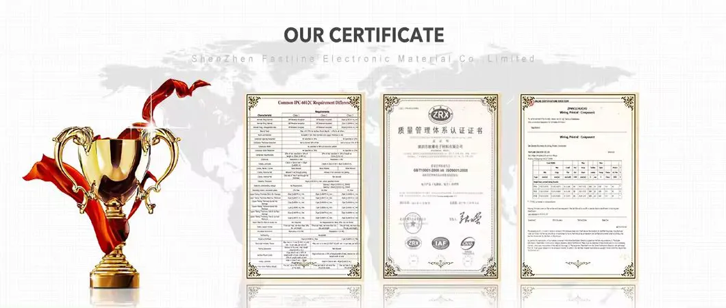
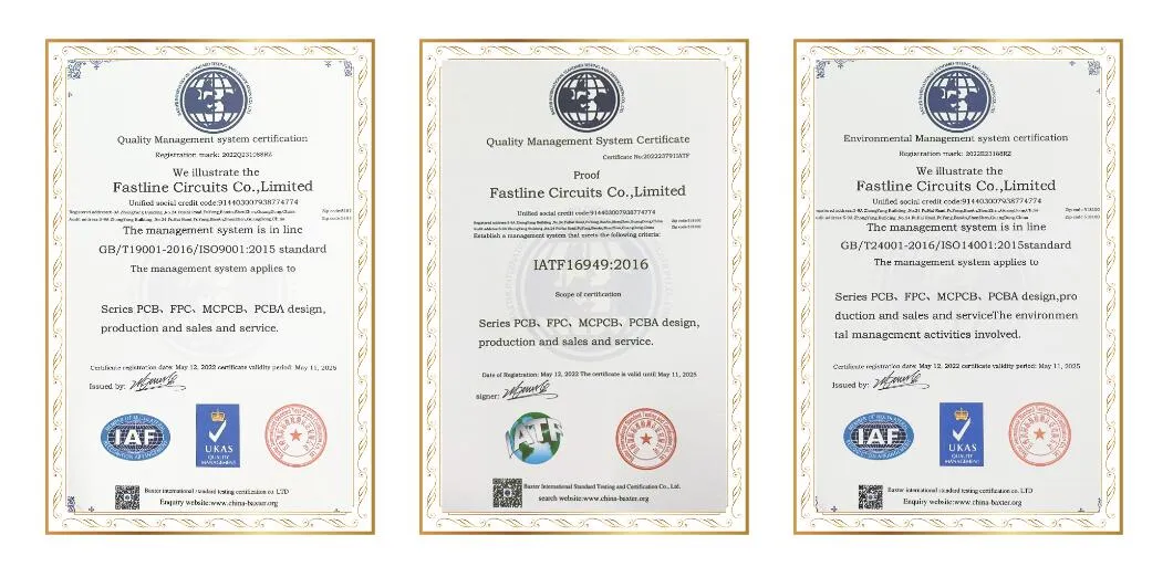
Certification UL, RoHS, ISO9001: 2000, ISO14000: 2004, SGS
Testing Flying probe, E-TEST, X-RAY Inspection, AOI
Files Supported Gerber, Protel, DXP, Auto CAD, PADS, OrCAD, Express PCB, etc.
Certifications
Certification 1
Certification 2
Customers
-- Our Customers --
Customers Logo Cloud
Packaging & Shipping
-- Packing and Shipping --
Packaging Detail
Shipping Detail
PCB Prototype Lead Time:
Item (Layers) General Time Quick Turn
1-2 Layers 4 days 1 day
4-6 Layers 6 days 2 days
8-10 Layers 8 days 3 days
12-16 Layers 12 days 4 days
18-20 Layers 14 days 5 days
22-26 Layers 16 days 6 days
Note: Based on all complete and problem-free data received. Lead time indicates ready-to-ship status.
Frequently Asked Questions
Q Do you have an order minimum?
We accept orders with as low as a quantity of 1 (piece or panel).
Q What kind of transportation do you adopt?
It will depend on your choice. We regularly ship via DHL if you don't have special requirements, as it is very fast and safe.
Q How long does it take to receive the product?
For mass production, products are typically shipped in 10 to 15 days. For PCB samples, delivery takes 5 to 7 days after all Gerber data is verified by our engineering team. For PCBA projects, delivery is within 5 to 7 days after the PCB fabrication process is complete.
Q What are the lead times for quick-turn prototypes?
Quick-turn prototype options are available as fast as 1 day for 1-2 layers, 2 days for 4-6 layers, and up to 6 days for complex 22-26 layer boards.
Q What is your manufacturing layer capability?
We support professional PCB manufacturing ranging from 1 up to 26 layers, including HDI (2+N+2) capabilities.
Q How do I place an order?
Please submit your detailed inquiry, and we will issue a Proforma Invoice for your order review.
One-Stop PCB & PCBA Solution
One-Stop Solution Overview

Related Products